RESEARCH
ELECTRONIC AND OPTICAL PROPERTIES OF SEMICONDUCTOR NANOSTRUCTURES
- Details
- Category: RESEARCH
 Electronic and optical properties of semiconductor nanostructures (well, wire, and dots) are studied by applying both envelope function approximation and full band approaches such as tight-binding and pseudopotentials. Our research cover the following areas:
- Strained quantum well (GaN, InGaAsP, AlGaAs etc.)
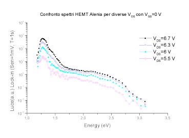
- Si, GaN nanowires
- AlGaAs/GaAs quantum wires
ELECTRONIC DEVICE SIMULATIONS
- Details
- Category: RESEARCH
 High electron mobility transistors (HEMTs) and heterojunction bipolar ransistors (HBTs) based on GaAs, GaN, InP are the most widely used microwave devices for low noise and power applications. We performed both Monte Carlo and Drift-Diffusion approaches to investigate:
- Impact-ionization regime
- Reliability
- RF response
FABRICATION AND MEASUREMENT ACTIVITIES
- Details
- Category: RESEARCH
 OLABs is mainly involved in the fabrication and measurement of optoelectronic and electronic devices based on organic semiconductors. Two main activities are under development: the fabrication of organic and hybrid organic/inorganic solar cells and the fabrication of Carbon Nanotube based field emitters. OLABs is part of MINAS for the development of micro and nanostructured devices and CHOSE for the study and fabrication of organic solar cells.
NITRIDE BASED SEMICONDUCTOR
- Details
- Category: RESEARCH
 Gallium Nitride and related material are wide band gap semiconductor suitable for light emitters in the green-ultraviolet region and for high power microwave transistors. Our theoretical investigation deals with:
- Optical and electronic properties of nitride nanostructures
- Screening of polarization fields
- Nitride LASERs and LEDs
- Nitride-based high electron mobility transistors
OPTOELECTRONIC DEVICE SIMULATIONS
- Details
- Category: RESEARCH
 Active and passive optoelectronic devices are the backbone of optical communication systems. With a variety of simulation tools, ranging from sophisticated Monte Carlo analysis to beam propagation methods, we perform:
- Modeling of semiconductor optical amplifiers, optical switches and lasers
- Full band calculation of optical gain (tight-binding, pseudopotentials)
- Theoretical study of dynamical properties based on rate-equation approaches
ORGANIC AND MOLECULAR ELECTRONICS
- Details
- Category: RESEARCH
 Organic materials and molecules have been proposed as alternative to conventional inorganic semiconductors for opto and microelectronic applications. Our activity concentrates on Thiophene, Porphyrines and PPV organic materials. We use ab-initio as well as empirical methods to study:
- Non-equilibrium transport
- Structural and optical properties
- Excited states in molecular crystals
QUANTUM CASCADE LASERS
- Details
- Category: RESEARCH
 Electronic Quantum Cascade Lasers (QCLs) have been demonstrated as the only valuable semiconductor light source for far-infrared application in the range 4-11 mm and up to THz range. We theoretically investigate the electron dynamics in QCLs, both for the InGaAs/AlInAs and for the GaAs/AlGaAs systems. The foolowing tools are used for this investigation:
- Monte Carlo analysis
- Quantum transport
QUANTUM TRANSPORT
- Details
- Category: RESEARCH
 Modern nanostructured devices have typical dimensions of few nanometers. Carrier transport in such structures can no longer be described by semiclassical theories. We have developed a variety of quantum approaches ranging from density matrices to non-equilibrium Green functions to describe:
- Transport in nanometric electronic devices such as CNT- FET and SiNW-FET
- Zener tunneling and Bloch Oscillations
- Resonant Tunneling Diodes
TECHNOLOGY CAD
- Details
- Category: RESEARCH
 A proper analysis of the optical and transport properties of semiconductor nanostructured devices requires sophisticated multiscale simulators. They should account, on equal footing, the atomistic details of the nanostructured active region as well as the macroscopic details of the whole device (contacts, strain, potential etc.). To this end OLAB is developing the multiscale Technology CAD called TiberCAD.
Several features are considered in this tool:
- 3D drift-diffusion for electron, holes and excitons
- Strain, piexo and pyro polarization
- Tight-binding models (empirical and DFT) for the atomistic description